Associated Faculty & Staff

Dr. Vijaya Kumar Gurugubelli
Faculty

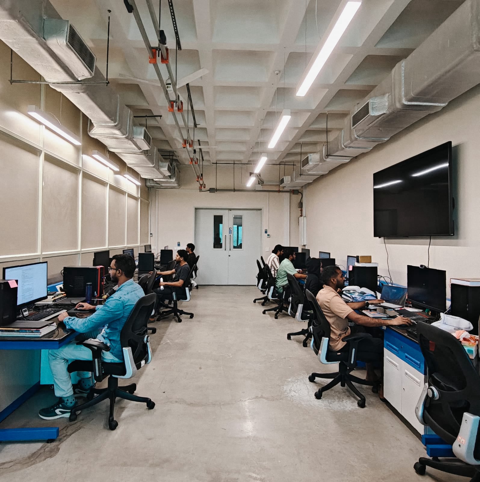
About the Lab:
The Device Simulation Lab focuses on understanding and designing next-generation semiconductor devices through advanced computational modeling. Using state-of-the-art TCAD, quantum transport solvers, and multiphysics tools, we study nanoscale charge transport, material behavior, and device performance in emerging transistor architectures.Our work spans CMOS scaling, 2D-material FETs, tunneling devices, and novel nanoelectronic structures. By combining physics-based simulations with material and process modeling, the lab provides insights that guide experimental development and enable innovations in faster, energy-efficient electronic technologies.
Key Research Areas:
>Analytical and Compact Modeling
>Power Semiconductor Devices
>Theoretical and Computational Nanoelectronics
>Boundary Value Problems
>Circuit Design with Novel Materials and Devices
>Sensors
Software tools include:
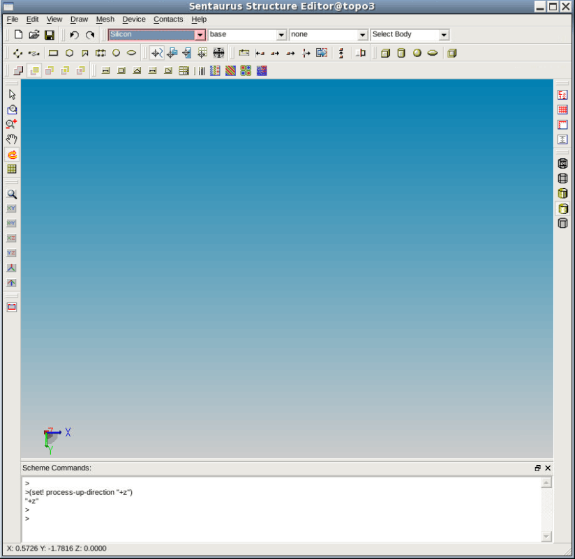
AsiaPac Advanced TCAD University Bundle
> 3-year TSL network license
> Floating license
> Number of licenses: 5
Synopsys QuantumATK – Materials and Device Simulation (with NEGF)
> Standard Academic Bundle
> 5 floating licenses of QuantumATK (DFT / semi-empirical) with NEGF
> 5 floating licenses of ATK Master Force Field (classical)
> 2 licenses of VNL (GUI)
> 2 licenses of VNL Links (VASP interface)
> 256 MPICH slave cores for accelerated simulations
All licenses are deployed on a single cluster.
Publication(s):
> P. N. S. Bhargav and V. K. Gurugubelli, “Modeling and optimal design of silicon superjunctions considering charge imbalance,” *Semiconductor Science and Technology*, vol. 40, no. 5, 055014, 2025.
> P. N. S. Bhargav and V. K. Gurugubelli, “On the need for accurate experimental determination of the impact ionization coefficients along ⟨1120⟩ direction in 4H-SiC,” *2024 IEEE 11th Workshop on Wide Bandgap Power Devices & Applications (WiPDA)*, 2024.
> V. K. Gurugubelli and P. N. S. Bhargav, “Enhanced theoretical lower limit for the specific on-resistance of a silicon balanced superjunction,” *IEEE Transactions on Electron Devices*, vol. 71, no. 6, pp. 3823–3830, 2024.
> A. V. N. Devi, P. N. S. Bhargav, S. Khandelwal, V. K. Gurugubelli, and S. Karmalkar, “Numerical simulation and parameter extraction of pure thermionic emission across Schottky contacts,” *2022 IEEE International Conference on Emerging Electronics (ICEE)*, pp. 1–5, 2022.
> V. K. Gurugubelli and S. Karmalkar, “An integral equation approach to model the drastic change in depletion width from bulk to nanoscale junctions,” *IEEE Transactions on Electron Devices*, vol. 65, no. 4, pp. 1493–1501, 2018.
> V. K. Gurugubelli and S. Karmalkar, “Effective medium theory based analytical models for the potential and field distributions in arrays of nanoscale junctions,” *Journal of Applied Physics*, vol. 122, no. 2, 2017.
> S. Jain, V. K. Gurugubelli, and S. Karmalkar, “An analytical model of the frequency-dependent 3-D current spreading in forward biased shallow rectangular pn junctions,” *IEEE Transactions on Electron Devices*, vol. 64, no. 2, pp. 507–514, 2017.
> V. K. Gurugubelli, R. C. Thomas, and S. Karmalkar, “Corrections to ‘An analytical model of the DC and frequency-dependent 2-D and 3-D current spreading in forward-biased shallow pn junctions,’” *IEEE Transactions on Electron Devices*, vol. 63, no. 5, p. 2223, 2016.
> V. K. Gurugubelli and S. Karmalkar, “Effective medium theory of the space-charge region electrostatics of arrays of nanoscale junctions,” *Journal of Applied Physics*, vol. 119, no. 2, 2016.
> V. K. Gurugubelli and S. Karmalkar, “Analytical theory of the space-charge region of lateral pn junctions in nanofilms,” *Journal of Applied Physics*, vol. 118, no. 3, 2015.
> V. K. Gurugubelli and S. Karmalkar, “Vertical nanowire array Schottky junction — A new power rectifier concept,” *73rd Device Research Conference (DRC)*, 2015.
> V. K. Gurugubelli, R. C. Thomas, and S. Karmalkar, “An analytical model of the DC and frequency-dependent 2-D and 3-D current spreading in forward-biased shallow pn junctions,” *IEEE Transactions on Electron Devices*, vol. 62, no. 2, pp. 471–477, 2014.
> V. Kumar Gurugubelli and S. Karmalkar, “A unified analytical model of the junction electrostatics in nanowire and nanotube arrays,” *Applied Physics Letters*, vol. 104, no. 20, 2014.
> V. K. Gurugubelli and S. Karmalkar, “A scalable curve-fit model of the substrate coupling resistances for IC design,” *13th International Symposium on Quality Electronic Design (ISQED)*, pp. 353–357, 2012.
> S. Karmalkar, K. R. K. Maheswaran, and V. K. Gurugubelli, “Ambient field effects on the current–voltage characteristics of nanowire field-effect transistors,” *Applied Physics Letters*, vol. 98, no. 6, 063508, 2011.
> S. Karmalkar, V. K. Gurugubelli, and K. R. K. Maheswaran, “Effect of the drain configuration on the current-voltage characteristics of vertical nanowire field-effect transistors,” *International Conference on Solid State Devices and Materials (SSDM)*, 2011.
> V. K. Gurugubelli, J. Vijayan, and S. Karmalkar, “Current-voltage characteristics of nanowire junctions,” *International Workshop on the Physics of Semiconductor Devices (IWPSD)*, 2011.
TCAD
Device Simulation Lab
© Copyright 2024 Department of Electrical Engineering,
IIT TIRUPATI - All Rights Reserved.
Developed by Dept. of Electrical Engineering, IIT Tirupati.