Associated Faculty & Staff

Prof. N V L Narasimha Murty
Faculty
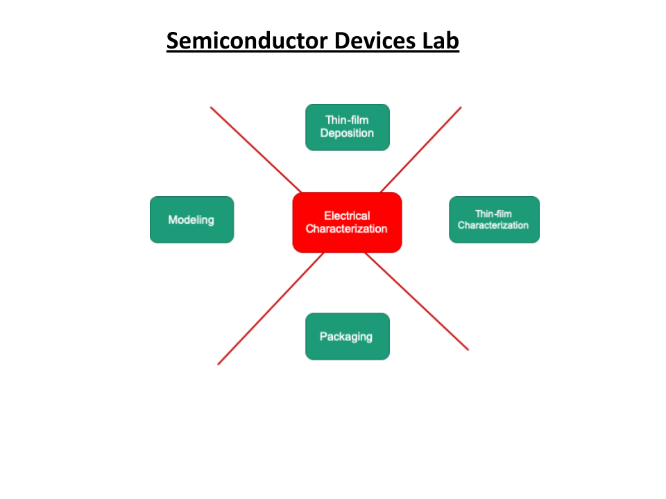
About the Lab:
The Semiconductor Devices Lab was established in the year of 2018. The lab primarily caters to the needs of undergraduate, master and doctoral students in the broad area of Semiconductor Devices and Nanoelectronics.
Key Research Areas:
>Defect identification and characterization in semiconductors (Diamond, SiC)
>Reliability of Semiconductor Devices
>Thin-film sensors
>Sensors for harsh environments
>Electrochemical soil sensors fabrication and characterization
>Ferroelectric devices, memories fabrication and characterization
>Radiation effects in semiconductors
>wide-bandgap semiconductors
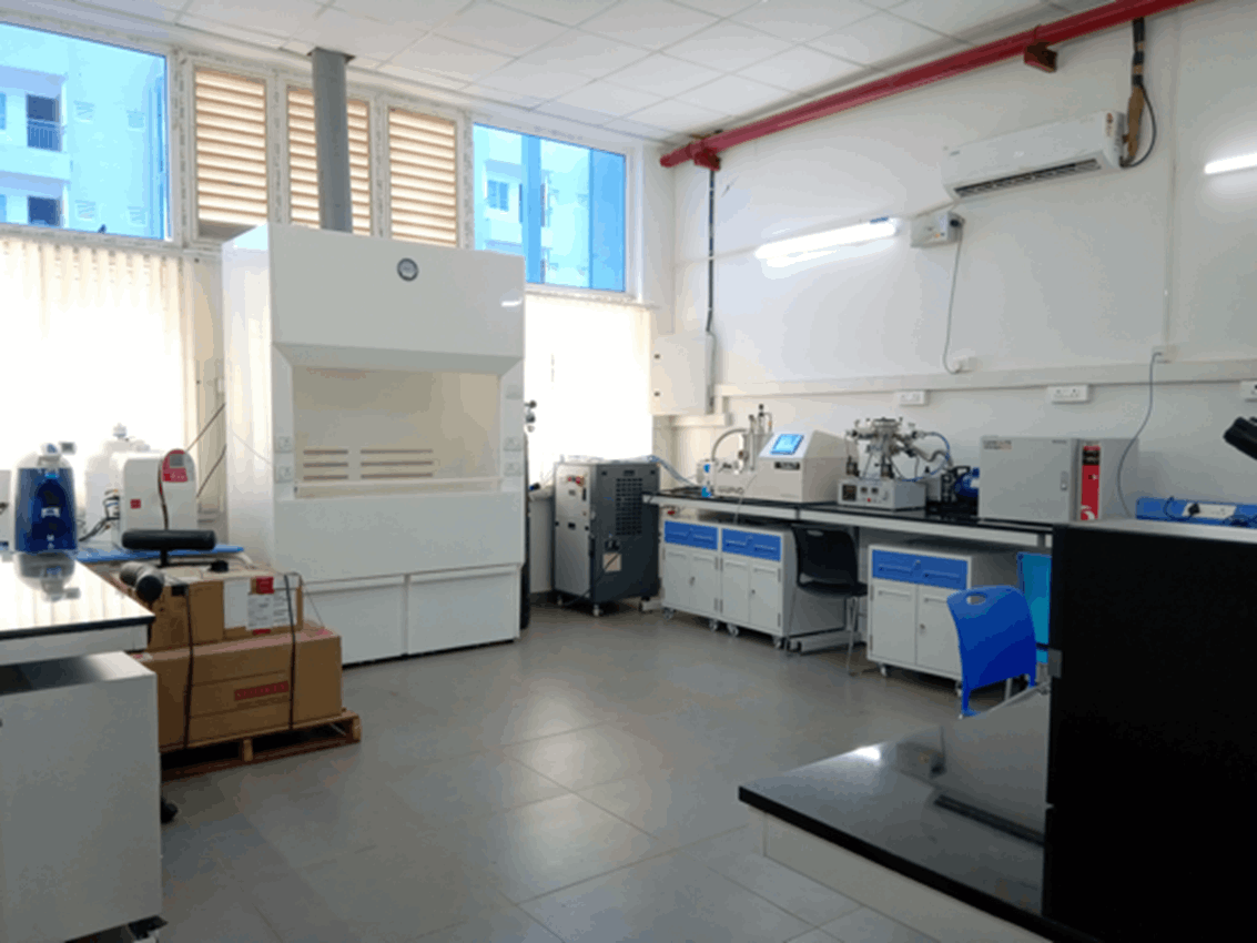
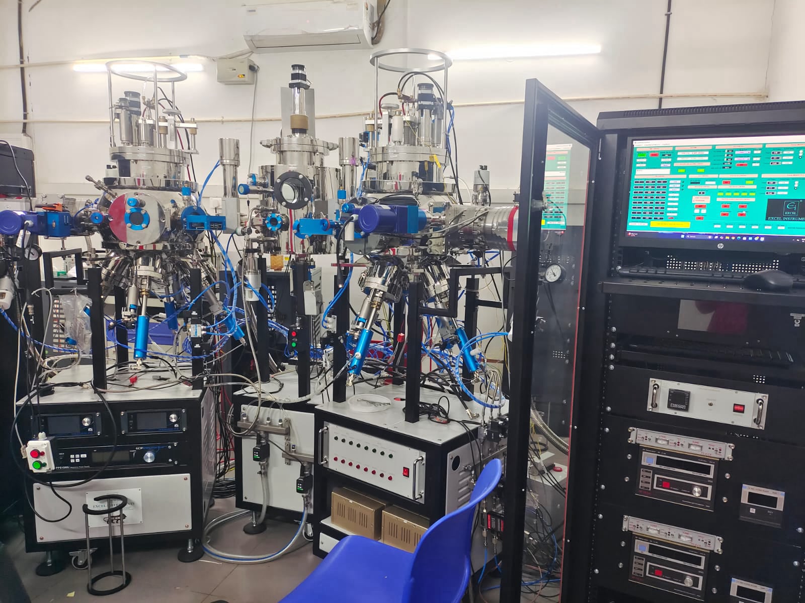
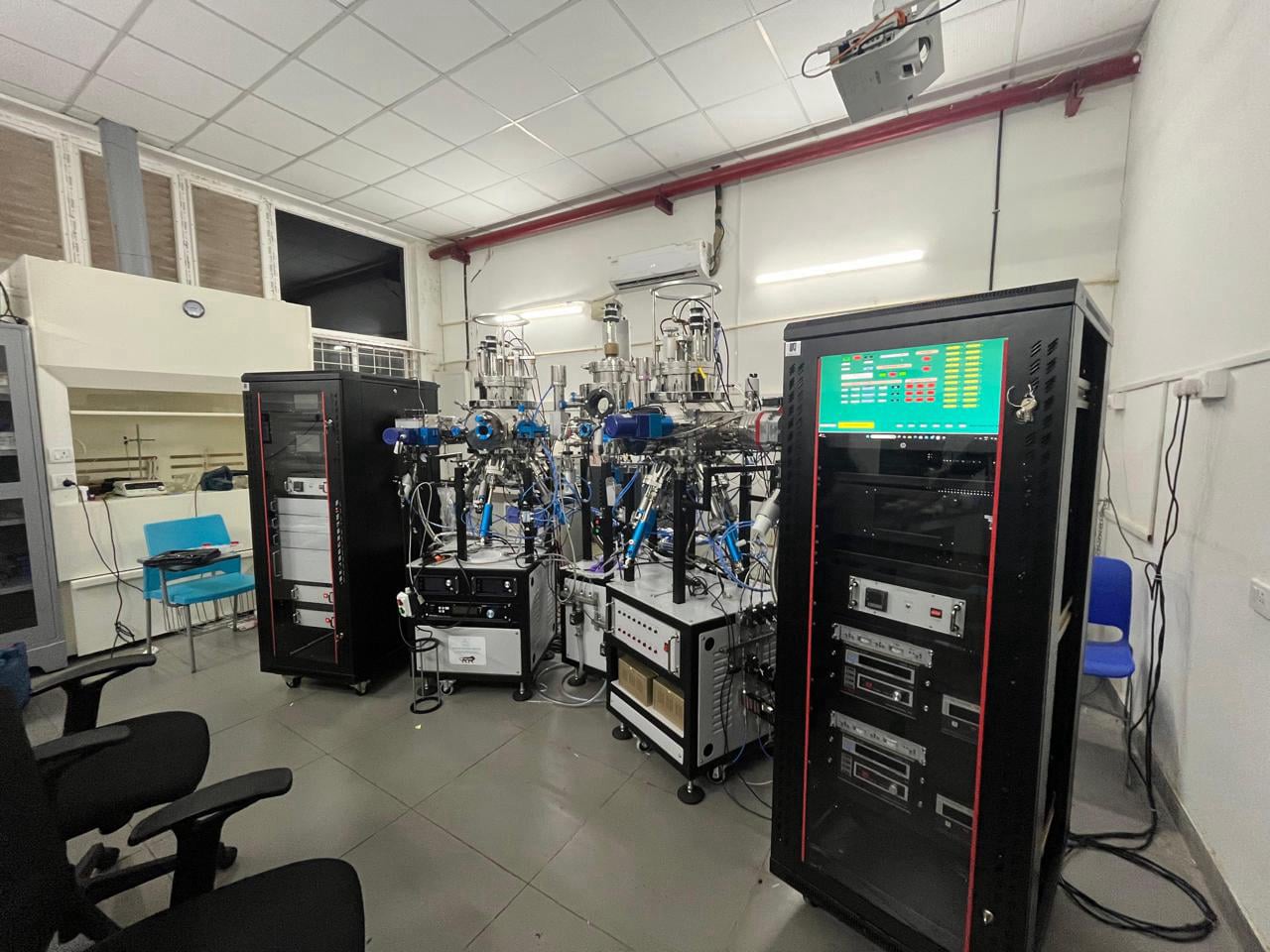
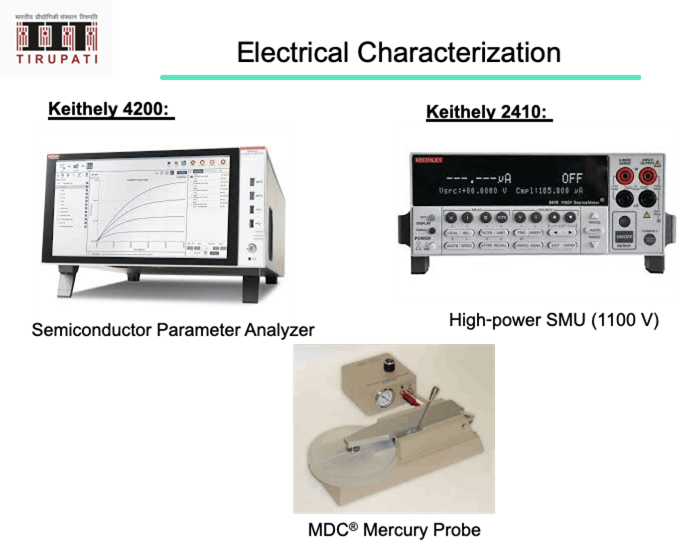
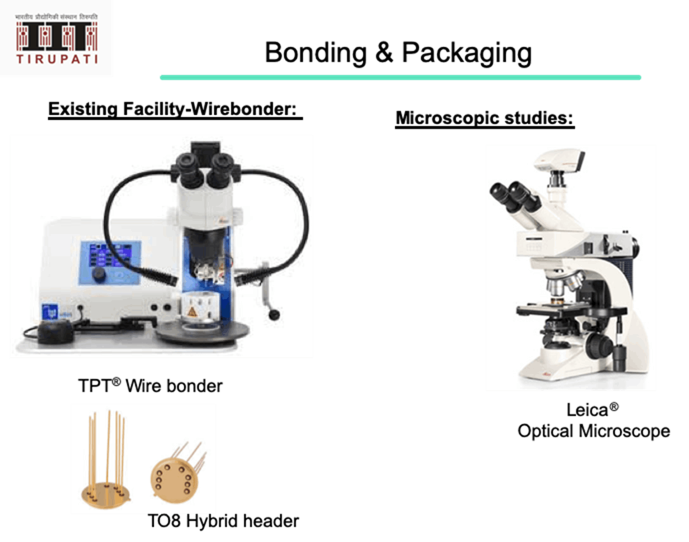
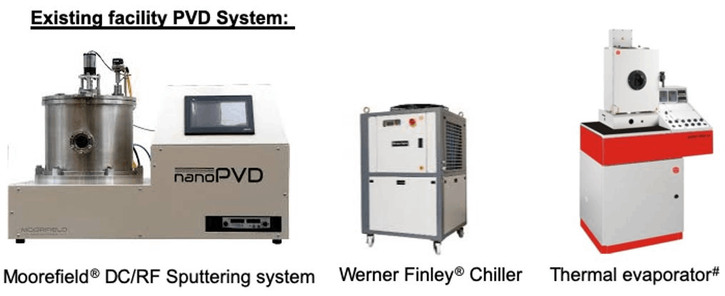
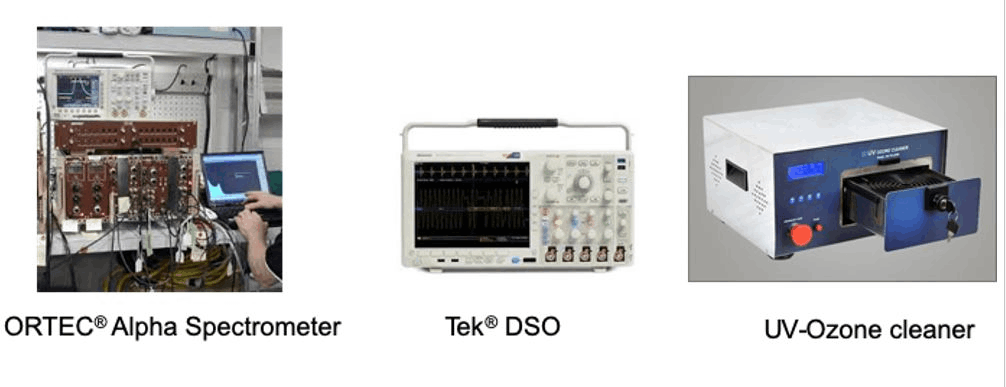
List of the Equipment(s):
■ Table top wire bonder (Bench-top thermosonics wire bonder for Wedge 7 Ball bounds)
■ Table top DC/RF sputtering unit with accessories
■ Gas test chamber
■ Bench top Oven
■ Hot Plate with Magnetic stirrer
■ Semiconductor parameter analyzer
■ Mercury probe station with accessories
■ Clean room compatible wet chemical bench
■ Ultrasonic bath with heater mech basket
■ Water purification system
■ Spin coating unit with UV Curing system
■ Thermal evaporation system tailored for organic thin films
■ Table top wirebonder (Bench-top thermosonics wire bonder for Wedge 7 Ball bounds)
■ Table top DC/RF sputtering unit with accessories
■ Gas test chamber
■ Bench top Oven
■ Hot Plate with Magnetic stirrer
■ Semiconductor parameter analyzer
■ Mercury probe station with accessories
■ Clean room compatible wet chemical bench
■ Ultrasonic bath with heater mech basket
■ Water purification system
■ Spin coating unit with UV Curing system
■ Thermal evaporation system tailored for organic thin films
Publication(s):
> S. Mohapatra, M. Abhangi, S. Vala, P. K. Sahu, NVLN Murty, “Characterization of electrically and optically active defects in synthetic single-crystal diamond-based radiation detectors,” *Journal of Electronic Materials*, 1–9, 2025.
> SZ Yousuf, S. Mamilla, NVLN Murty, “Enhanced resistive switching in dopant-free BFO devices via TiO₂ insertion,” *IEEE Transactions on Materials for Electron Devices*, 2025.
> S. Mamilla, SZ Yousuf, M. M. Avulapati, A. Al-Mallahi, NVLN Murty, “A low-cost, reusable all-solid-state TiN-based EGFET soil pH sensor,” *IEEE Sensors Journal*, 2024.
> A. Shilpa, NVLN Murty, “Alphavoltaic performance of 4H-SiC Schottky barrier diodes,” *IEEE Transactions on Nuclear Science*, 2024.
> C. H. N. Raghuram, G. K. Kumar, V. Sreeja, C. Tharani, A. Vivaswanth, …, “Efficient approximate adder design for image brightness enhancement: Balancing area, power, and delay,” *2024 International Conference on Computer, Electronics, Electrical Engineering*, 2024.
> S. Mamilla, SZ Yousuf, M. M. Avulapati, A. A. Mallahi, NVLN Murty, “Planar Ag/AgCl reference electrode for electrochemical agronomic sensors,” *IEEE Sensors Letters* 8(7), 1–4, 2024.
> S. Kumari, R. Singh, S. Kumar, NVLN Murty, D. Planson, C. Raynaud, …, “Electrical characteristics and trap signatures for Schottky barrier diodes on 4H-SiC, GaN-on-GaN, AlGaN/GaN epitaxial substrates,” *Semiconductor Science and Technology* 39(6), 065016, 2024.
> A. B. Yadav, NVLN Murty, B. Lasya, S. Mamilla, B. S. Sannakashappanavar, “Density functional theory-based study of Ag/ZnO Schottky diode,” *Journal of Electronic Materials* 52(5), 3228–3241, 2023.
> G. N. K. Reddy, M. S. Manikandan, NVLN Murty, L. R. Cenkeramaddi, “Unified quality-aware compression and pulse-respiration rates estimation framework for reducing energy consumption and false alarms of wearable PPG monitoring devices,” *IEEE Access* 11, 41708–41740, 2023.
> A. Shilpa, S. Singh, NVLN Murty, “Spectroscopic performance of Ni/4H-SiC and Ti/4H-SiC Schottky barrier diode alpha particle detectors,” *Journal of Instrumentation* 17(11), P11014, 2022.
> V. L. Vineela, P. A. Praveen, T. Kanagasekaran, N. Kumar, NVLN Murty, “Direct X-ray detection using thin-film pentacene Schottky diodes,” *Journal of Instrumentation* 17(02), P02024, 2022.
> B. S. Sannakashappanavar, A. B. Yadav, V. Kumar, NVLN Murty, K. Singh, “Low resistance ohmic contact on ZnO thin film revealed by Schottky barrier height,” *Silicon* 14(4), 1531–1536, 2022.
> G. N. K. Reddy, M. S. Manikandan, NVLN Murty, “Evaluation of objective distortion measures for automatic quality assessment of processed PPG signals for real-time health monitoring devices,” *IEEE Access* 10, 15707–15745, 2022.
> G. N. K. Reddy, M. S. Manikandan, NVLN Murty, “Information theoretic metrics for automatic quality assessment of processed PPG signals,” *2021 3rd International Conference on Electrical & Electronic Engineering*, 2021.
> G. N. K. Reddy, M. S. Manikandan, NVLN Murty, “Predictive coding with simultaneous extraction of pulse and respiration rates from PPG signal for energy constrained wearable devices,” *2021 4th International Conference on Bio-Engineering for Smart Technologies*, 2021.
> G. N. K. Reddy, M. S. Manikandan, NVLN Murty, “Performance of spectral, autocorrelation and peak count based PR estimation methods under normal/abnormal PPG for wearable devices,” *2021 IEEE International Conference on Health, Instrumentation & Measurement*, 2021.
> G. N. K. Reddy, M. S. Manikandan, NVLN Murty, “Lightweight compressed sensing (CS) and partial DCT based compression schemes for energy-efficient wearable PPG monitoring devices,” *2021 IEEE International Conference on Health, Instrumentation & Measurement*, 2021.
> S. Mohapatra, M. Abhangi, S. Vala, P. K. Sahu, S. Rath, NVLN Murty, “Comparative study of single crystal (SC)-diamond and 4H-SiC bulk radiation detectors for room temperature alpha spectroscopy,” *Journal of Instrumentation* 16(06), P06020, 2021.
> B. S. Sannakashappanavar, A. B. Yadav, C. R. Byrareddy, …, “Synthesis of ZnO ultra-thin film-based bottom-gate phototransistors for UV detection,” *Journal of Electronic Materials* 49(9), 5272–5280, 2020.
> S. Mohapatra, P. K. Sahu, S. Rath, P. K. Sahoo, S. Varma, NVLN Murty, “Impact of nitrogen induced defect dynamics on UV response of diamond photodetectors,” *Superlattices and Microstructures* 142, 106504, 2020.
> S. Mohapatra, P. K. Sahu, S. Rath, NVLN Murty, “Defect characterization and numerical modeling of single-crystal ultra-pure intrinsic diamond,” *Diamond and Related Materials* 106, 107822, 2020.
> G. N. K. Reddy, M. S. Manikandan, NVLN Murty, “On-device integrated PPG quality assessment and sensor disconnection/saturation detection system for IoT health monitoring,” *IEEE Transactions on Instrumentation and Measurement* 69(9), 6351–6361, 2020.
> S. Mohapatra, P. K. Sahu, NVLN Murty, “Characterization and TCAD simulation studies of single-crystal diamond detectors,” *International Conference on Computers and Devices for Communication*, 2019.
> B. S. Sannakashappanavar, A. B. Yadav, C. R. Byrareddy, NVLN Murty, “Fabrication and characterization of Schottky diode on ultra-thin ZnO film and its application for UV detection,” *Materials Research Express* 6(11), 116465, 2019.
> P. Raja, NVLN Murty, “Thermally annealed gamma-irradiated Ni/4H-SiC Schottky barrier diode characteristics,” *Journal of Semiconductors* 40(2), 022804, 2019.
> G. N. K. Reddy, M. S. Manikandan, NVLN Murty, “Integrated data compression and pulse-rate extraction scheme using differential coding for wireless PPG monitoring devices,” *2018 IEEE International Conference on Industrial and Information Systems*, 2018.
> S. Mohapatra, P. K. Sahu, NVLN Murty, “Numerical modeling of native defects in CVD-grown diamond photodetectors,” *2018 IEEE Electron Devices Kolkata Conference (EDKCON)*, 198–201, 2018.
> P. Raja, NVLN Murty, “Thermal annealing studies in epitaxial 4H-SiC Schottky barrier diodes over wide temperature range,” *Microelectronics Reliability* 87, 213–221, 2018.
> D. Vigneshwara Raja, NVLN Murty, “Thermally stimulated capacitance in gamma-irradiated epitaxial 4H-SiC Schottky barrier diodes,” *Journal of Applied Physics* 123(16), 2018.
> P. Raja, J. Athira, C. V. S. Rao, S. M. Abhanga, NVLN Murty, “D–T neutron and ⁶⁰Co-gamma irradiation effects on HPSI 4H-SiC photoconductors,” *IEEE Transactions on Nuclear Science* 64(5), 958–965, 2017.
> P. Raja, J. Athira, C. V. S. Rao, S. M. Abhanga, NVLN Murty, “Spectroscopic performance studies of 4H-SiC detectors for fusion alpha-particle diagnostics,” *Nuclear Instruments and Methods in Physics Research A*, 2017.
> P. M. Raja, J. Athira, C. V. S. Rao, M. Abhangi, NVLN Murty, “Performance of epitaxial and HPSI 4H-SiC detectors for plasma X-ray imaging systems,” *Journal of Instrumentation* 12, P08006, 2017.
> P. Raja, NVLN Murty, “Electrically active defects in neutron-irradiated HPSI 4H-SiC X-ray detectors investigated by ZB-TSC technique,” *IEEE Transactions on Nuclear Science* 64(8), 2377–2385, 2017.
> P. Raja, C. V. S. Rao, NVLN Murty, “Numerical simulation of ⁶⁰Co-gamma irradiation effects on electrical characteristics of n-type FZ SiC detectors,” *Nuclear Instruments and Methods in Physics Research B*, 2016.
> P. Raja, NVLN Murty, “Investigation of X-ray spectral response of DT fusion-produced neutron irradiated PIPS detectors for plasma X-ray diagnostics,” *Journal of Instrumentation* 10(10), P10018, 2016.
> P. Raja, NVLN Murty, “An improved analytical model of 4H-SiC MESFET incorporating bulk and interface trapping effects,” *Journal of Semiconductors* 36(3), 034004, 2016.
> P. Raja, NVLN Murty, C. V. S. Rao, M. Abhangi, “Effect of DT fusion-produced neutron irradiation on X-ray spectral characteristics of PIPS detectors,” *2014 IEEE Radiation Effects Data Workshop (REDW)*, 1–4, 2014.
> NVLN Murty, “The role of substrate compensation on DC characteristics of 4H-SiC MESFET with buffer layer: A combined two-dimensional simulations and analytical study,” *Materials Science Forum* 778, 887–890, 2014.
> NVLN Murty, “Unlocking the potential of wide bandgap semiconductors for harsh environments,” *AIP Conference Proceedings* 1576(1), 19–21, 2014.
> M. H. L. Rao, NVLN Murty, “An improved IV model of 4H-SiC MESFETs incorporating substrate trapping, surface trapping and thermal effects,” *2013 Spanish Conference on Electron Devices*, 75–78, 2013.
> NVLN Murty, M. H. L. Rao, “Analytical study of substrate parasitic effects in common-base and common-emitter SiGe BHT amplifiers,” *Journal of Microwaves, Optoelectronics and Electromagnetic Applications* 12, 2013.
> NVLN Murty, S. M., “A new semi-empirical model for the backgating effect on the depletion width modulation in GaAs MESFETs,” *Journal of Semiconductor Technology and Science* 8(1), 104–109, 2008.
> NVLN Murty, S. M., “A new analytical model for photo-dependent capacitances of GaAs MESFETs with emphasis on the substrate-related effects,” *Solid State Electronics* 50(11–12), 1716–1722, 2006.
> NVLN Murty, S. M., “Static IV characteristics of optically controlled GaAs MESFETs with emphasis on substrate-induced effects,” *Journal of Semiconductor Technology and Science* 6(3), 211, 2006.
> NVLN Murty, S. M., “Analytical study of photo-effects on common-source and common-drain microwave oscillators using high pinch-off n+-GaAs MESFETs,” *Microelectronics Journal* 37(5), 452–458, 2006.
> NVLN Murty, S. M., “A photo-dependent capacitance model of GaAs MESFETs,” *Physica Status Solidi A* 203(5), 1005–1017, 2006.
> NVLN Murty, S. M., “Analytical modelling of photo-effects on the S-parameters of GaAs MESFETs,” *Microwave and Optical Technology Letters* 48(1), 150–155, 2006.
> NVLN Murty, S. M., “An analytical model for the S-parameters of optically controlled GaAs MESFETs,” *2005 Conference on Electron Devices*, 103–106, 2005.
> M. V. Rao, NVLN Murty, “Early lung cancer detection using radial basis function neural networks (RBFNN),” *International Journal of Modern Trends in Engineering and Research*, 2005.
> P. V. Raja, C. V. S. Rao, NVLN Murty, “Electrical characteristics and UV response of 4H-SiC Schottky diodes and bulk photoconductors,” *IEEE Transactions on Nuclear Science* 52(6), 2005.

© Copyright 2024 Department of Electrical Engineering,
IIT TIRUPATI - All Rights Reserved.
Developed by Dept. of Electrical Engineering, IIT Tirupati.